Brick Breaker

So I decided to pick my game development hobby back up.  It’s been a while, about 15 years.  Video games are actually why I started programming.  In high school I wanted to make games and during summer break I’d stay up till morning working on them every night.  I’ve still got that old code, well most of it.  It’s horribly out of date though.  So I’ve started re-writing some of my old shared code to target modern APIs.  To kick it off I started with something simple, a brick breaker clone.  I could have used an existing engine to do this in a fraction of the time, but I’ve always been fascinated with engine development, so I did it from scratch.  Here’s a few things I learned along the way.

X11 Fullscreen
I was creating a window that covered the screen with override redirect on to do fullscreen.  This works, but it’s the “old” way of doing it and I also wanted to toggle fullscreen on the fly.  It’s feasible to toggle override redirect and move the window around to cover the screen.  This is basically how I’m doing it on windows.  But there’s a better way.  There is a property named _NET_WM_STATE that contains a list of window states.  Setting the list with XChangeProperty to the _NET_WM_STATE_FULLSCREEN atom makes the window fullscreen and removing the property with XDeleteProperty makes the window normal.  What’s nice about this approach is the window manager is involved instead of being bypassed.  The window manager will pick the right monitor for you and automatically restore the old window position/size when exiting fullscreen.

GTK+ Fullscreen
GTK+ conveniently has a fullscreen mode, which probably uses _NET_WM_STATE.  However it won’t make the window fullscreen if it’s not resizable, which makes sense, but I want my window to have a fixed size until it’s fullscreened so I can control the aspect ratio.  Simple fix though: just set gtk_window_resizable to true before using gtk_window_fullscreen right?  Yes and no, the problem is that resizable doesn’t change immediately so you have to wait for it to sync with the window manager.  My solution was to set resizable then set fullscreen and pump the message queue in a loop until fullscreen actually changes.  I’d rather use a function that syncs changes with the window manager, but I haven’t found one yet.  One problem with this is that the window manager is allowed to ignore the fullscreen request.  So I’ll only try for a second before assuming the window manager denied my request.  I could possibly wait for the resizable property to change instead of the fullscreen property, but I’m concerned that the property will change before it’s synced with the window manager.

DMG “Installer” and .DS_Store
Dmgs (Disk Images) are a pretty great way to redistribute Macos applications.  Users just have to drag and drop the application bundle, no installer necessary.  The dmg has a link to the applications folder so it’s easy to copy and it even has a nice background image.  There are plenty of guides online for how to create a dmg file manually, but I wanted to create one from a script.  No problem, I’ll use hdiutil to create a dmg from a folder.  But that alone doesn’t work, the background doesn’t show up.  Why doesn’t this work?  I don’t know what kind of black magic goes on in .DS_Store files, but the background image is apparently not just a relative path to the file.  You have to create a writable dmg file, create your template .DS_Store file with the dmg mounted, and copy it to your staging area.  Trying to create the .DS_Store file in your staging area won’t work.  The dmg guides tell you to do this of course, but not why, so unless you know about the .DS_Store magic you may assume, as I did, that any old .DS_Store file will do.  Ultimately I manually created a template .DS_Store file and put it in source control so I could create the dmg file from a script with this template file.

Dynamic Library Symbol Visibility in Macos
The symbol visibility for libraries is hidden by default on Macos, more specifically that’s the clang default in XCode.  This is great actually, since it means you don’t pollute your executable with symbols from your libraries.  But it’s not what I was expecting fresh from the Linux port, which defaults to visible.  Setting the visibility to default actually makes it visible, so the default visibility on Macos is not “default”.  I didn’t catch this right away because the Debug build worked fine, and if it worked then what madness is it that the Release build doesn’t work.  Well the debug build has testability on by default, which apparently also affects symbol visibility (so test code can access “internal” functions I assume).  I flipped this option and my Release build started working.  In the future I’ll probably set the visibility attribute in gcc/clang similar to how I use declspec dllexport/dllimport in msvc.

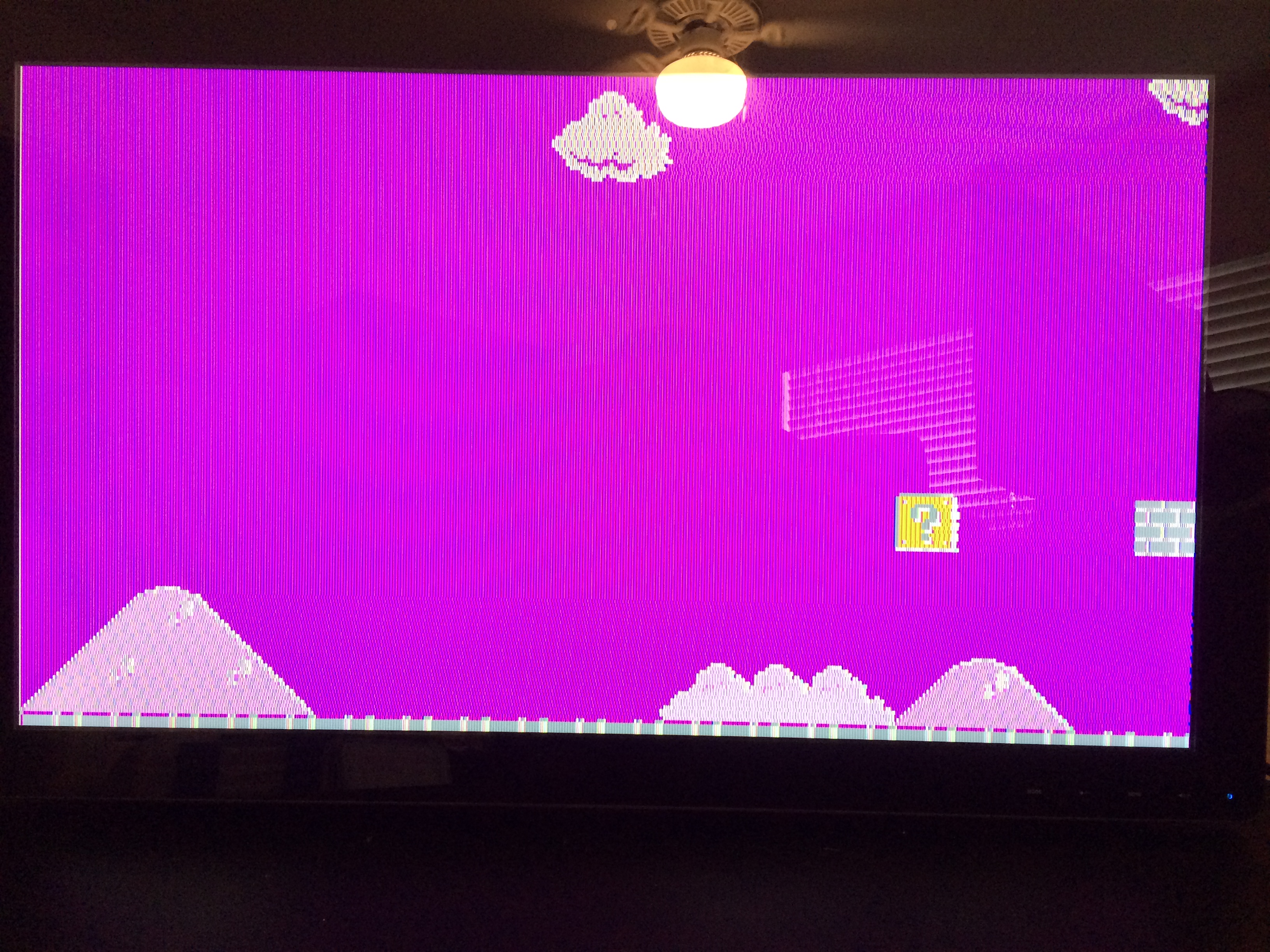
And now a screenshot:

Thrilling, absolutely thrilling.

A Galleria of Failure

Plus a modicum of success.  Let’s start with the more interesting of the two, glitches.  This first one is is actually the first image I got with the board.  Here the data going to the dvi serializes was bit swapped, causing all the colors to be wrong.

pink image

Here is a video of the glitch I mentioned in a previous post.  This actually turned out not to be a glitch in the logic clock as I originally thought.  What was happening is the frame and line start pulses are generated off the dvi clock and then cross to the logic clock domain.  Both pulses happen on the same clock in the dvi domain and the logic domain expects the frame start pulse to occur at or before the first line start pulse.  But for some reason the frame start pulse would cross one clock after the line start pulse.  This prevents the map pointer from resetting to the beginning of the map data.  Instead the map pointer just kept incrementing, into uninitialized data.  I moved the frame start pulse one line back to fix it.

These next images are side effects of me fussing with the SRAM controller trying to get rid of the above glitch before I realized what was going on.  I basically re-wrote the controller a few times with varying ratios of registered and combinational logic.  I ended up sticking mostly with my original registered design, but with the SRAM clock shifted 180 degrees out of phase.

Video Glitch 1

Video Glitch 2

Video Glitch 3

And lastly here’s a video of everything mostly working.  Boring I know.  I’m scrolling the map with a SNES controller (the config interface is working now) and the audio unit is also playing a midi in the background, so the delta sigma DAC is confirmed working.  The audio is quiet so it’s hard to hear, deal with it.

Lessons learned: metastability is a pain, even if compensated for crossing clock domains isn’t perfect.  Gotta pack those IOBs.

Back on track

Back on main project. I’ve got firmware that compiles, so it’s time to order the boards. Whlie I’m waiting for them to arive I start tweaking on my video unit. I found a way to double it’s performance, all I have to do is add another clock. This should be fine, I already had that clock hooked up to a PLL. But wait, what’s this, a new and interesting error message I’ve not seen before. My clocks are unroutable, but how. As suggested by the most useful information source ever, some random person on some random forum, I tried compiling without my pin constraints file and it works. So once again I have run into a pin assignment error. What I don’t get is why it didn’t show up until I added this clock but that input clock is plugged into a PLL instance. Surly you know what comes next, to the data sheets! Hmm, the data sheet says clock networks are complicated and you should verify complex designs with the compiler. Well [explitive deleted]. After many hours of carefully studying the data sheet and making random changes to the code I came to the conclusion that the second PLL wasn’t actually being used. Because of the frequencies I was using and the fact that I wasn’t changing the phase of the clock I didn’t strictly need a PLL, just a clock doubler. So instead of using the entire PLL block I instanced the compiler picked a few other misc clock resources. To fix it I’d need to swap a few signals and move the clock input a few pins over so it could be routed to the second PLL because the clock input pins can only be routed to one of the PLLs. While I was working this out, the boards arived.

20140704-145446-53686815.jpg

20140704-145447-53687152.jpg

20140704-145447-53687521.jpg

Time for some hardware verifacation. I plugged it in and it didn’t burst into flames, I’m off to a good start. DVI works, it’s actually running at a higher frequency this time. I’m outputting a 720p60 image this time using the built in serializers, pixel doubled from 360p60. I tried it before and after making the board mod. Before the mod I saw some glitches that looked like they were in the logic clock domain. Like it would use the wrong level data periodicly. I suspected the clock I’m using (which is from the microcontroller) may not be stable enough. A PLL can, and did, clear that right up. I haven’t tested the audio DAC yet, but it’s low risk. The FPGA lives, so does it’s config memory. The FPGA can access the SRAM just fine. Though I am running it a little slower than I hoped I would. I suspected this might be the case, I was trying to run it almost at it’s maximum theoretical speed ignoring propagation delays. I don’t have any tricks up my sleve to improve this, but I’ve heard other people have tricks up their sleves that may help. If I can just get them to lend me their coats maybe I can find the tricks up their sleves and use them. The MCU debug port (USB to UART bridge) works, both spare RS323 UARTS work. The MCU can read the config dip switch and access the SD card. The MCU joystick port 1 works fine, joystick port 2 is acting like it’s got a solder bridge, but I haven’t found one. The FPGA debug pins are working (and quite useful).

While ckecking this I ran into another problem. My debugger stopped working entirely, I had to update it’s firmwre to get it to work unreliably. My JTAG programmer works once and then stops. My logic analyzer works on one USB port for a few times and then I have to switch to another port. And even my USB serial adapter is hit and miss. Why… because windows 8. I tried to press the screw it start over button. My favorite thing about windows 8, and it didn’t work. It said I had missing files. Why… because I upgraded from 7 to 8 then 8 to 8.1? It asks me to insert install media, which I don’t have because I upgraded instead of buying a full disk. How do I fix this, do I have to buy another copy of windows just to get the full install disk. I downgraded to windows 7 and now my USB devices are reliable again. As an added bonus the Xilinx tools crash less now too. Wonderful.

Now on to the MCU to FPGA to SRAM interface. This worked fine as an async pass through, but with the SRAM controller and arbiter in the loop it doesn’t. I output the control signals on the FPGA debug pins and probed them, nothing. So I output the clock on the debug pins and hooked it up to the scope, because checking the clocks is now a mandatory part of my diagnostic procedure. Bingo, it’s changed frequency, but why? The debugger is running, it changes when the debugger is running and then switches back when it’s not. That makes sense I guess, the debugger takes over and supplies it’s own clock. But it’s also a problem, and an important little detail I haven’t found in the data sheets. When the clock changes like that the PLL loses lock. So how do I fix this. Two ideas come to mind, mod the board adding another oscilator. Feed that oscilator into both the FPGA and the MCU. I like that solution, but it takes a board rev, or maybe I can solder on the oscilator dead bug style. Another option, feed the locked and reset signals into the MCU and have it reset the PLL when it looses lock. This will work and redefining a few signals or bodging then in is doable, but it has the side effect of resetting some of the logic along with the PLL. It’s a problem, but one I can work around until I can rev the board. I need the MCU and FPGA running off the same clock so the FPGA can register signals on the MCU to FPGA memory interface reliably. With this change the MCU can access the SRAM reliably, next up is getting the MCU to access the video and audio unit config interface. And that brings us up to date.

Lessons learned: FPGA clock networks are complicated. Sometimes you just can’t win.

A different set of rails

About two months ago I was once again sidetracked by another project. I had a very specific problem. I have two software protection keys from the same company for two different sets of software. This company unfortunately didn’t have the foresight to make these two keys compatible. So I had to physically remove one key and insert the other key to get the software to work. This was getting tedius and in a process I’ve otherwise been able to automate.  A quick search on my favorite parts site, digikey, shows a few USB hub ICs and I know there are USB microcontrollers around.  This is a problem I can solve. Get a hub, connect one port to the USB microcontroller, the other ports can go to the devices, then have the microcontroller recieve commands via USB to power the other two ports on and off. I looked for an existing commercial solution, but what I found went the other way. Selecting one USB devices between mutliple PCs instead of selecting between multiple USB devices connected to one PC. I might could have found an existing device if I looked harder, but life is a journey, rock it. And so I present to you this thing I made.

Raw Board

Assembled

It’s pretty simple, I just followed the reference design for the USB hub and whacked in the smallest, cheapest USB microcontroller I could find, following it’s reference design as well. It’s a PIC16LF1454. Microchip even provides a driver framework which does most of the work for you and samples to get you running quick. Of course something has to go wrong. Murphy knows me well, sometimes I wonder if he is a benevelant being who knows I won’t learn anything if I don’t make mistakes. And Murphy does so want me to learn. The first problem I encountered is the debugger doesn’t work under windows 8, because… windows 8. I solved this by connecting to the debugger under Linux and updating the firmware. The next problem I encountered is that I couldn’t get windows to recognize the microcontroller after loading any of the samples. First I hooked up the microcontroller seperately, directly to the computer to debug just it. Windows sees the device but doesn’t recognize it when I run the debugger. I noticed I could output the clock on one of the pins and on a whim decedied to enable it and probe it on my scope. Oddly enough the output wasn’t the right frequency. Score one for dumb luck. It turns out the samples support using an internal and external oscilator. I had already verified the samples were set for the internal oscilator and the config bits were also set correctly. It turns out I had to add a few lines to change the internal oscilator frequency. Fixed that and now it’s running.

I hooked up the complete board with the new firmware and still no dice. I probed the USB hub and all the device power enable signals are deasserted, why, because all the the overcurrent signals are asserted. The microcontroller overcurrent signal I just plain screwed up. I connected the active low signal to ground, meaning it was asserted. Woops. The next issue was a few missing pullup resistors. The reference design calls out the power switch IC I’m using, but it didn’t include the pullup resistors. I didn’t check this against the power switch data sheet, which looking at now, clearly indicates they are required. Woops again. Luckily my top layer has a power pour so I can just scratch off the solder mask here and there, cut a trace, drop in a solder bridge, whack in a few resistors, and now all is well. I made those changes to the board, but I haven’t gotten new boards manufactured.

Lessons learned: trust your data sheets, but not blindly, verify them against other data sheets if possible. SC70-3 chips are hard to hand solder.

Now to get back on sidetrack

I decided that I had learned enough from my prototype board and that it was time to start working on the real board. A single board that would have everything on it, no need for a seperate FPGA board. This time I will compile everything before ordering the boards. I decided to start with the SPU, I can also test this with my Papilio. My initial goal was to basically put a midi file in shared memory and point the SPU at it. I started to write a midi file reader in VHDL, the state machine got complicated in short order. Looking at it, it started to look like a processor. Then I thought, why not implement it as a soft processor. And this is the point where I get sidetracked. I designed a 16-bit register based RISC CPU, implemented it in software, wrote an assembler, implemented it in VHDL, and started creating a C compiler. The soft processor worked well enough to output hello world over a UART and even output a sine wave through a memory mapped delta sigma DAC.

Though there were a few lose ends to tie up. I had a 32-bit 16.16 fixed point unit in the design with add/subtract/multiply/divide. The divide translates to a 48-bit integer divide and I saw VHDL has a divide operator. I didn’t expect it to work, surely it won’t make timing, doing the divide in a single cycle, but I also didn’t expect it to fail quite as badly as it did. It wouldn’t even compile. The Xilinx tools told me I was trying to use 125% of my available resources. Woops. Luckily removing the fixed point instructions dropped my resource utilization down to 60%. I still need to remove those instructions completely or re-implement them using multiple cycles. I also noticed a few instructions I hadn’t tested yet had bugs in them. Then there was the C compiler. I had a pre-processor, parser, syntax analyzer, and I had started on the semantic analyzer, but I still had to finish it and implement the code generator and optimizer. Of course I’d also want a debugger and perhapse this is getting out of hand. Looking at my FPGA resource utilization, after adding JTAG debugging, the video unit, and the SRAM controller, I may well run out of resources before I get everything implemented.

Time to shelve this, maybe pick it up later with a new project with the soft processor taking up the entire FPGA. I decided instead to greatly simplify the audio unit and go back to implementing it in VHDL. Now instead of trying to read a midi file it would just handle the audio channels, generating sine waves and mixing them, with the CPU doing the sequencing. This simpler design was implemented and tested without too much fanfare and once again I’m on track. I added in the video unit modified from my earlier VGA/DVI tests and the SRAM controller and everything compiles.

Lessons learned: dividing is hard.

Step 3: Profit?

The next phase should be profit, but instead this phase is spend lots of money on prototypes and dev tools. I found another Spartan 6 based dev board, the Mojo. It doesn’t have onboard SDRAM like the Papilio, so there are more IO pins available. I still would like to mess with the SDRAM on the Papilio Pro, but I need SRAM for this project. The extra IO pins let me hook up the SRAM as well as the MCU. The shield was just big enough to fit all the essentials. The MCU, SRAM, SD slot, audio jack, joystick port, DVI port, ICSP header, and debug uart header. Yes an ICSP port, that means an external programmer, but that gives me debugging support too. Totally worth it. No room for a second joystick or RS-232 driver for the debug uart or config dip switch. The Mojo provided the FPGA and power. I designed the board and got it manufactured by OSH Park. I really dig the gold on purple color scheme and the boards have been high quality.

Raw board

Assembled

After assembly it’s time to verify the hardware. Joystick port worked fine, I ported the Arduino sketch easily enough. The audio DAC was a simple circuit and my previous test code worked fine on the new board. Then I got to the SD card. That was not so easy. I found a spec for the SPI interface to SD cards and implemented it. After banging my head for a while I turned off the music and looked for a better spec. I eventually found one with a timing diagram. I do so appreciate timing diagrams. It showed an extra 8 clocks not mentioned in the text for the SPI section. I later found a mention of the extra clocks in the SD protocol portion of the document, apparently this also applies to the SPI protocol. Alright, problem solved. I tried the code and it still doesn’t work. I check, double check, and triple check the traces going to the card. I would just happen to have those signals going through a few vias, so I soldered in a few bodge wires strait through the vias. Checked the signals with my logic analyzer, and they looked fine. After some more checking I eventually determined the SD slot had a broken solder joint. When I checked it I pressed down on the pin slightly, just enough for it to make contact with the pad. I re-soldered the pins and all is once again well.

At least until I tried the DVI port. I hooked it up to the differential pins nearest the DVI port up to it. The Xilinx tools were kind enough to tell me I had an error in my pin mapping. Odd it worked fine when I did something similar on the Papilio board. 80s style montage of me digging through the data sheets again and apparently not every differential pin can be used as input and output. I would just happen to pick at random pins that would work on the Papilio board. Luckily I would just happen to have a few unused pins that would work. Bodgewire to the rescue again. I carefully cut the traces so they’d all be the same total copper length from the FPGA (because they’re differential pairs of course) and soldered them on. I also had to swap out the audio pins. It’s not pretty, but I modified my VGA test to output DVI instead and it works. Unfortunately I can’t layout a new board. The signals I need for the DVI port cut off the signals I need to route for the audio jack. I can’t get around it without adding more layers to the board or using a jumper wire. So not actually impossible, but probably not worth the time.

Bodgewire

I checked the UART earlier, sure it works. Then I moved onto the SRAM. It also did not work. Lots of long traces of differing length. I figure I can get it to work at a lower speed, not ideal. Then I realize the LED array on the Mojo is also connected to the shield pins and those pins are used for the RAM. I found that in the schematic, I appreciate that they provided it, open hardware and all, but I wish they also mentioned the LEDs were hooked up like that in the documentation. Ohh well, but that’s probably messing with my rise and fall times, so I desolder the resistor array leading to the LEDs, destroying the resistor array and pullling up one of the pads in the process. Still it does not work. At this point I made the command decision to goof off and play video games.

Lessons learned: that surface mount SD slot is hard to solder, not much I can do about it other than to stop being such a filthy casual and get good at soldering. FPGA pins have different capabilities, check every pins capability in the data sheet. FPGAs have multiple data sheets, much like the pokemons, you have to find them all. Check your pin mappings with test code, the compiler can catch your errors.

But will it blend?

Next phase is proof of concept and feasibility checks. I started with an Arduino. I’m really glad to see this device on the market. The last time I looked into simple hobbyist microcontrollers the BASIC STAMP was what you could easily get. I like the Arduino because you program it in C instead of it being a microcontroller running a BASIC interpreter. They’re pretty close to using a microcontroller directly but easier to use and still very capable devices. Anyways, I picked up an Arduino and googled the NES/SNES/Genisis controller pinout and protocol. That was pretty strait forward to get working. I also picked up an SD card shield, which also worked without much trouble.

The next thing I wanted to check out was the FPGA. I picked up a Papilio Pro along with a logic start megawing. This is another great board. That board and the intro to Spartan FPGA book got me rolling quickly. If you want to learn how to use an FPGA I can’t recommend those two enough. The Papilio Pro has a Xilinx Spartan 6 FPGA which is the chip I decided to use because of it’s IO count and popularity with the hobbyist community. I seriously had no idea it was going to be this easy, while also being this hard. The type system in VHDL is actually a pain, it took me months to get it under control. Pro tip: use qualified expressions. I was tempted more than once to learn Verilog just to get away from VHDLs type system.

My first task was to blink LEDs, print hello world out a UART, and many other simple things you do when first learning hardware. My first real task was to generate a VGA signal. This was surprisingly simple with equal parts “wait that’s all there is to it” and “wait, what, you can’t do that.” All async, level memory indexing into tile memory, tile memory wired strait to the VGA pins. Crude, but it worked. Then on to audio, a counter indexing a sine rom, outputting to a delta sigma DAC on the Pailio board. Around then I read of another fellow getting DVI output working on the Spartan 6 chip. Turns out generating a DVI signal isn’t to terribly more complicated then generating VGA. It has a higher refresh rate at the same resolution, so it will take more memory bandwidth. On the other hand I don’t actually have any 4:3 TVs that will take NTSC, everything is 16:9. DVI is also electrically compatible with HDMI and I figure I can generate a much higher quality 480p signal compared to 480i. That and the delta sigma DAC means I can drop the video encoder and audio DAC from the design. The delta sigma DAC isn’t nearly as good as the I2S audio DAC I was going to use, but the trade off for a simpler design is worth it. I even generated a crappy, unstable, hacked together DVI signal from the Papilio.

Lessons learned: even simple equations can take more than a clock to propagate, powers of 2 are key, bit concatenation is king.

8 bits are plenty

I’ve decided to restart my website blog type thing to document a project I’ve been working on for over a year now. The next few posts will recap my project(s) since then.

It all started with a friend of mine saying how surprised he was that the TurboGrafx-16 had some decent looking games even though it only had an 8-bit processor. I took this as a slight upon 8-bit processors everywhere. Modern 8-bit microcontrollers being quite powerful. So I decided to create a modern 8-bit game console with 16-bit like capabilities and see what it can do with it. That’s cheating of course, comparing an old 8-bit CPU to a modern one, but I don’t care. Plus I hadn’t done any board design, so this will be new and interesting.

My first thought was to use a microcontroller to generate an NTSC signal. Some googling showed this was possible and had sucessfully been done before, but in each case the signal generated was, well, crappy. It’s impressive people have been able to get it to work at all, but the signal is either monocrome or low resolution. A microcontroller just isn’t fast enough to generate a full resolution color image without some external help. For instance a common frequency for providing data to an NTSC encoder is 27MHz, but the Atmel chip I settled on runs at 32MHz. That doesn’t leave any room for generating meaningful data. I needed something with lots of horsepower and accurate timing. What do you do when you need that, you get an FPGA. Another thing I hadn’t done before, more new and interesting. So I could have a microcontroller controlling an FPGA that feeds data to an external NTSC video encoder.

I’ll also need to make some noise. I’d already settled on an FPGA at this point, so I might as well have it also act as the SPU. I found some audio DACs using I2S, which is apparently a thing, and also awesome. I also considred using a seperate microcontroller with I2S or build in audio DACs. The ones I found either didn’t have as much memory as I calculated I’d need, or they were 32-bit. And that’s just too many bits, that’s cheating. The specific kind of cheating that I won’t do, or is it? The 68k in the Genisis looks like a 32-bit processor from software, even though it’s implemented with a 16-bit core. I’ll also need joysticks. I have a handful of NES/SNES/Genisis controllers in my collection I can use. Next up I’ll need a “cartrige.” Micro SD cards are ubiquitous and I’ve seen them interfaced with an Arduino before via SPI. So that will work.

I’ll also need more cowbell RAM. And this is where it gets messy. You need lots of signals to get RAM running. I have to consider what can I reasonably manufacture without it becoming prohibitively expensive for a hobby project. How many layers the board can have, what IC packages I can use. I can’t hand solder BGA, that would have to be professionally manufactured. Fully assembled one-off prototype boards are too expensive for me to stomach. 2-4 layer boards are relatively cheap to get manufactured and TQFP chips are hand solderable. Ideally I’d like to have seperate RAMs for the CPU and GPU/SPU with the GPU/SPU mapped into the CPU’s memory space. That poses three problems, routing that many signals on a relatively low density board, having enough pins in the FPGA, and finding a CPU with a flexible memory controller. There’s the Atmel chips with expandable data memory, Microchip chips with expandable program memory, and Zilog cips (makers of the venerable Z80) with expandable program and data memory. Ideally I’d like to have expandable prgram and data memory, so the Zilog chip is the clear winner. But do I have enough pins? No, no, I do not. The most usable pins I can get in a TQFP FPGA is about 100. The FPGA->RAM interface takes about 45 signals, the CPU to FPGA interface takes about 45 as well, the FPGA to audio DAC interface takes about 4, the FPGA to video encoder interface takes about 10, and by the way some of those 100 pins are dual use and really ought to be used just for configuration.

Expandable program memory is interesting, but that makes mapping the FPGA into the CPU’s memory space not feasible becuase of how program memory is modified. thank’s modified hardvard architecture. Expandable data memory is what I really want, though it does mean I have to update the MCUs flash to load a new game from the “cartrige.” The Atmel chip also has an SDRAM controller as well as an SRAM controller that can be used simultaniously with the SRAM controller having multiplexed signals so it uses fewer pins. This is awesome and perfect and only available on a variant of the chip they don’t sell and requires an SDRAM chip that’s not manufactured anymore. So my dream of having seperate RAMs just isn’t happening. The FPGA will have to demultiplex the MCU signals and act as an arbiter between the MCU/GPU/SPU and RAM. On top of this the Atmel chip’s memory controller doesn’t have an external wait signal, so I have to have fixed timing to the RAM, which limits me to an SRAM. The problem with trying to interface to DRAM from an SRAM interface is that DRAM requires refresh cycles. So the CPU needs to know it has to wait or be told to wait while this happens. Without a wait signal you have to assume the worse possible case (a DRAM refresh occurs right when the memory access is requested) and insert wait states to wait until the DRAM can respond. The worst case access time is 100 times slower than the typical access time. SRAM is easier to interface to, but much more expensive than DRAM and only available in smaller capacities.

So I’ve got a plan that will totally work and not have to change drastically.

And one more thing

Why the hell does MSI support the the standard 4 number W.X.Y.Z versioning scheme, and then ignore the last number in the version.  It apparently does it’s own thing for the last digit and that works fine for files, but it ignores the last number in package versions.  Packages don’t have anything to fill in for that last digit.  I use a major.minor.revision.build version scheme and I have to install new revisions of software with the version number the same except the build number.  It’s getting all confused because it can’t tell the difference between version 1.20.0.230 and 1.20.0.231 of the package.

Luckily I hardly ever reset the build number so I can swap the build and revision numbers and still get a unique version even if the last number is ignored.  So that’s what I’m gona do.  The build number is only incremented about twice a day, so at that rate I have to reset the build number once every 89 or so years.  I think that’ll do.

Snarfle the Garflonk

When did installing software become so damn complicated.  It used to be all you had to do was copy these files to this place and be done with it.  Actually for the most part that’s all you still have to do.  Of course Microsoft had to make it complicated in their MSI format.  I’ve been trying to move from NSIS to MSI using WiX and I still can’t get the whole put this file there thing working.

With NSIS it’s pretty easy to do, but that’s about it.  The “programming language” that NSIS uses is so primitive that it’s damn near impossible to do anything else.  You have to find someone who wrote a DLL that does what you want and then you have to piece together 20 lines of code just to call a function.  I know damn well the VM in NSIS is complete enough to support an actual language instead of that bastardized assembly like thing they use.  It’s all way too much work to do something really simple, something that would be just a few lines of C code.

An installer will inevitably have to call other installers to install it’s dependancies.  With NSIS you can at least do this, it’s not even possible with MSI.  Apparently the shit will hit the fan and all hell will break loose if you try to install an MSI file from within another MSI file.  Of course this was a feature Microsoft once touted then being able to do with MSI, and then they realized that it never worked right and caused all sorts of problems and forbade it’s use.  Just like most everything in the Win32 API that has a DWORD reserved parameter that must be NULL for NT but 42 for 9x.

The newest version of MSI will let you chain MSI files which is nice if all of your install stuff is strait MSI, which is never the case.  No-one distributes a plain MSI file; there’s always either a setup program with an embedded MSI file that you can’t get to, at least not without angering the computer gods, or there’s an MSI file with a bootstrapper.  So many MSI developers had to use a bootstrapper that they gave it a name and formal definition.  And why does one need a bootstrapper.  Because MSI can’t run other installers and therefore install dependancies, so you have to do it in an external program.

Wow, four whole paragraphs and I haven’t even gotten to what started this rant.  I’m trying to make an installer with WiX.  Don’t get me wrong though, I have a lot of respect for the WiX guys, and the NSIS guys as well.  But it’s bit a huge pain in the ass.  WiX exposes you to the soft squishy underbelly of MSI; which is as great as it is terrible.  If you’ve ever used a Windows box for more than just web surfing you’ll realize eventually that the soft squishy underbelly of anything that Microsoft does is a complicated mess.  And MSI is no exception.  I get the feeling if I were to sneeze too hard around MSI it would fall apart, cats and dogs would rain from the sky, start mating, and give birth to creatures God never intended to exist and for good reason.  Then my eyes would pop out, dangle there for a second, and then explode.  Not sure exactly why, maybe I left them open when I sneezed.

But, I digress; again.  The problem of the hour is that my WiX files are generating warnings like:

warning: L407: you forget to snarfle the garflonk

So I look up L407 and if I’m lucky enough it tells me how to snarfle the garflonk, else I google till my eyes bleed.  Eventually I manage to snarfle the garflonk.  And then I get this:

error: L408: you snarfled the garflonk

So I can never get it to compile without errors or warnings.  It seems that most of the files I have that compile with no errors, but with warnings go from anywhere between not installing  properly to to failing horribly.  Meanwhile the files that compile with errors and a few warnings in there for good measure seem to work just fine.

Just great.  I think the compiler is just garbage in, garbage out and will only fail if something horrendous happens.  Which isn’t an unreasonable thing to do.  Then they rely on the ICE validation scheme to produce all the errors and warnings.  But their implementation of ICE validation is teh suck.

Alright, I’m done.  You can go away now.