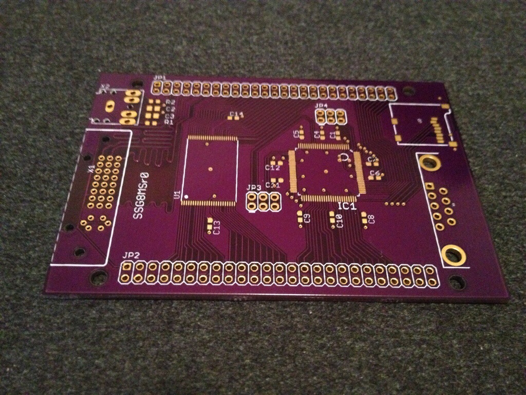
The next phase should be profit, but instead this phase is spend lots of money on prototypes and dev tools. I found another Spartan 6 based dev board, the Mojo. It doesn’t have onboard SDRAM like the Papilio, so there are more IO pins available. I still would like to mess with the SDRAM on the Papilio Pro, but I need SRAM for this project. The extra IO pins let me hook up the SRAM as well as the MCU. The shield was just big enough to fit all the essentials. The MCU, SRAM, SD slot, audio jack, joystick port, DVI port, ICSP header, and debug uart header. Yes an ICSP port, that means an external programmer, but that gives me debugging support too. Totally worth it. No room for a second joystick or RS-232 driver for the debug uart or config dip switch. The Mojo provided the FPGA and power. I designed the board and got it manufactured by OSH Park. I really dig the gold on purple color scheme and the boards have been high quality.

After assembly it’s time to verify the hardware. Joystick port worked fine, I ported the Arduino sketch easily enough. The audio DAC was a simple circuit and my previous test code worked fine on the new board. Then I got to the SD card. That was not so easy. I found a spec for the SPI interface to SD cards and implemented it. After banging my head for a while I turned off the music and looked for a better spec. I eventually found one with a timing diagram. I do so appreciate timing diagrams. It showed an extra 8 clocks not mentioned in the text for the SPI section. I later found a mention of the extra clocks in the SD protocol portion of the document, apparently this also applies to the SPI protocol. Alright, problem solved. I tried the code and it still doesn’t work. I check, double check, and triple check the traces going to the card. I would just happen to have those signals going through a few vias, so I soldered in a few bodge wires strait through the vias. Checked the signals with my logic analyzer, and they looked fine. After some more checking I eventually determined the SD slot had a broken solder joint. When I checked it I pressed down on the pin slightly, just enough for it to make contact with the pad. I re-soldered the pins and all is once again well.
At least until I tried the DVI port. I hooked it up to the differential pins nearest the DVI port up to it. The Xilinx tools were kind enough to tell me I had an error in my pin mapping. Odd it worked fine when I did something similar on the Papilio board. 80s style montage of me digging through the data sheets again and apparently not every differential pin can be used as input and output. I would just happen to pick at random pins that would work on the Papilio board. Luckily I would just happen to have a few unused pins that would work. Bodgewire to the rescue again. I carefully cut the traces so they’d all be the same total copper length from the FPGA (because they’re differential pairs of course) and soldered them on. I also had to swap out the audio pins. It’s not pretty, but I modified my VGA test to output DVI instead and it works. Unfortunately I can’t layout a new board. The signals I need for the DVI port cut off the signals I need to route for the audio jack. I can’t get around it without adding more layers to the board or using a jumper wire. So not actually impossible, but probably not worth the time.

I checked the UART earlier, sure it works. Then I moved onto the SRAM. It also did not work. Lots of long traces of differing length. I figure I can get it to work at a lower speed, not ideal. Then I realize the LED array on the Mojo is also connected to the shield pins and those pins are used for the RAM. I found that in the schematic, I appreciate that they provided it, open hardware and all, but I wish they also mentioned the LEDs were hooked up like that in the documentation. Ohh well, but that’s probably messing with my rise and fall times, so I desolder the resistor array leading to the LEDs, destroying the resistor array and pullling up one of the pads in the process. Still it does not work. At this point I made the command decision to goof off and play video games.
Lessons learned: that surface mount SD slot is hard to solder, not much I can do about it other than to stop being such a filthy casual and get good at soldering. FPGA pins have different capabilities, check every pins capability in the data sheet. FPGAs have multiple data sheets, much like the pokemons, you have to find them all. Check your pin mappings with test code, the compiler can catch your errors.